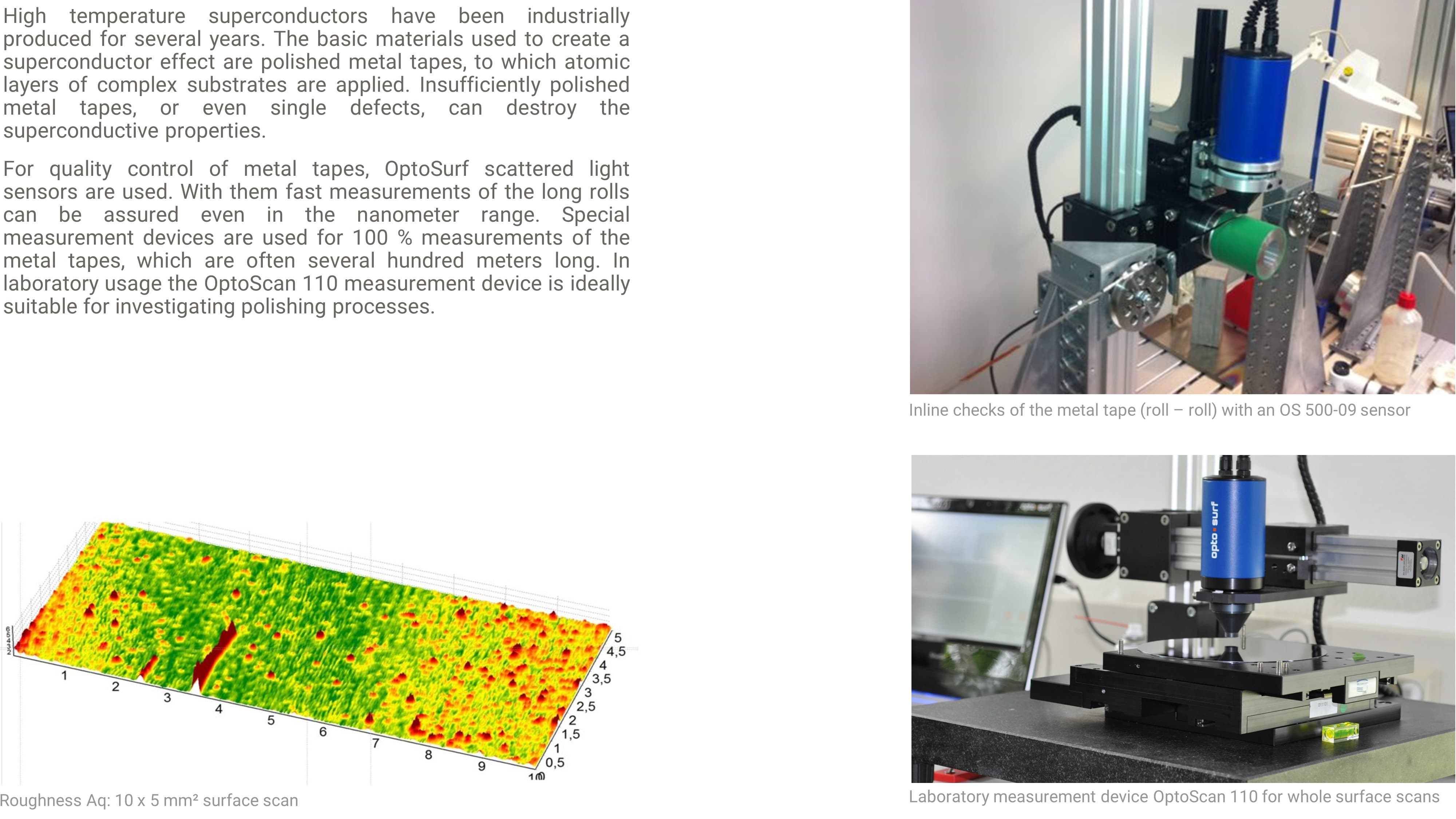
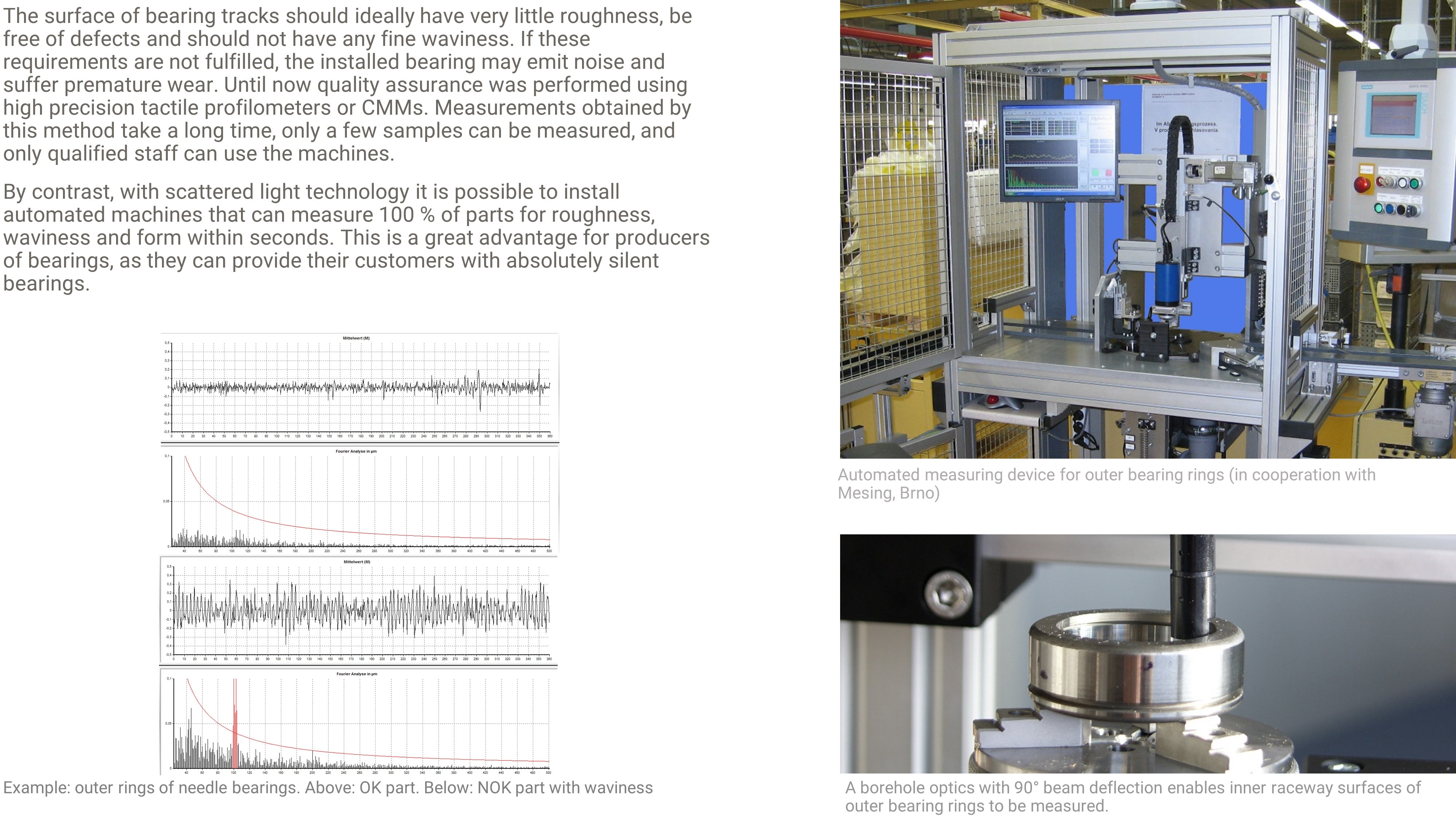
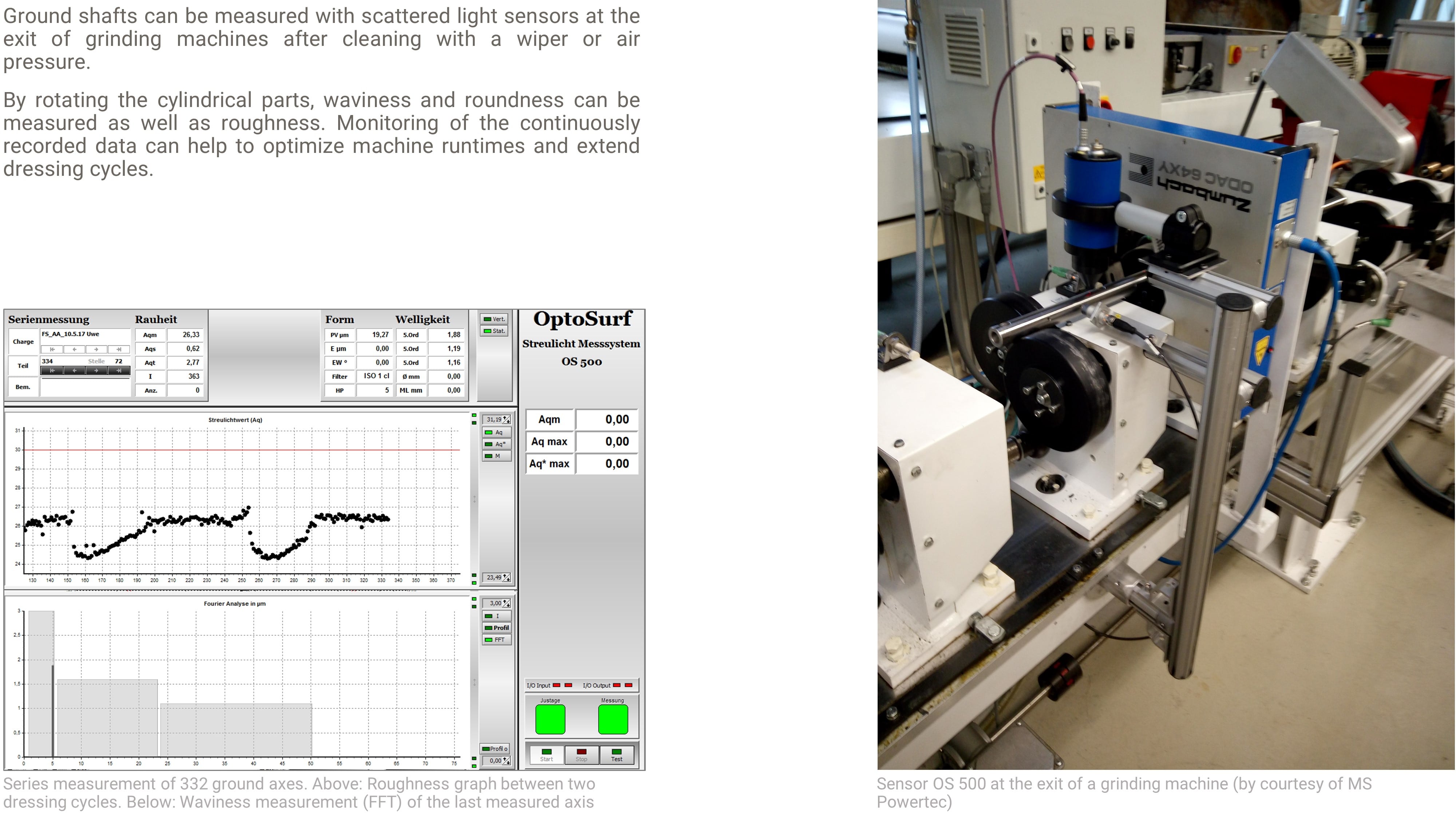
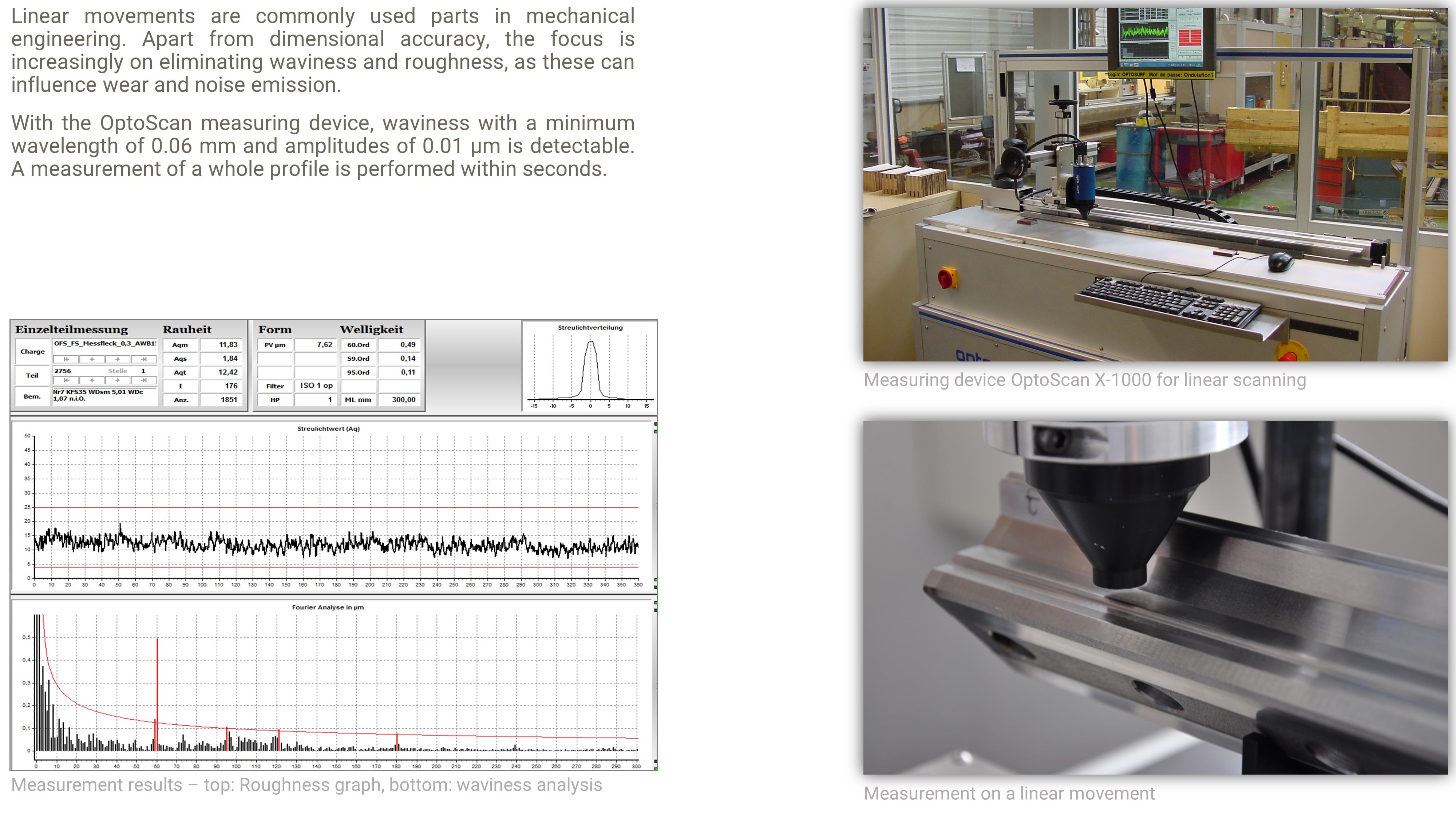
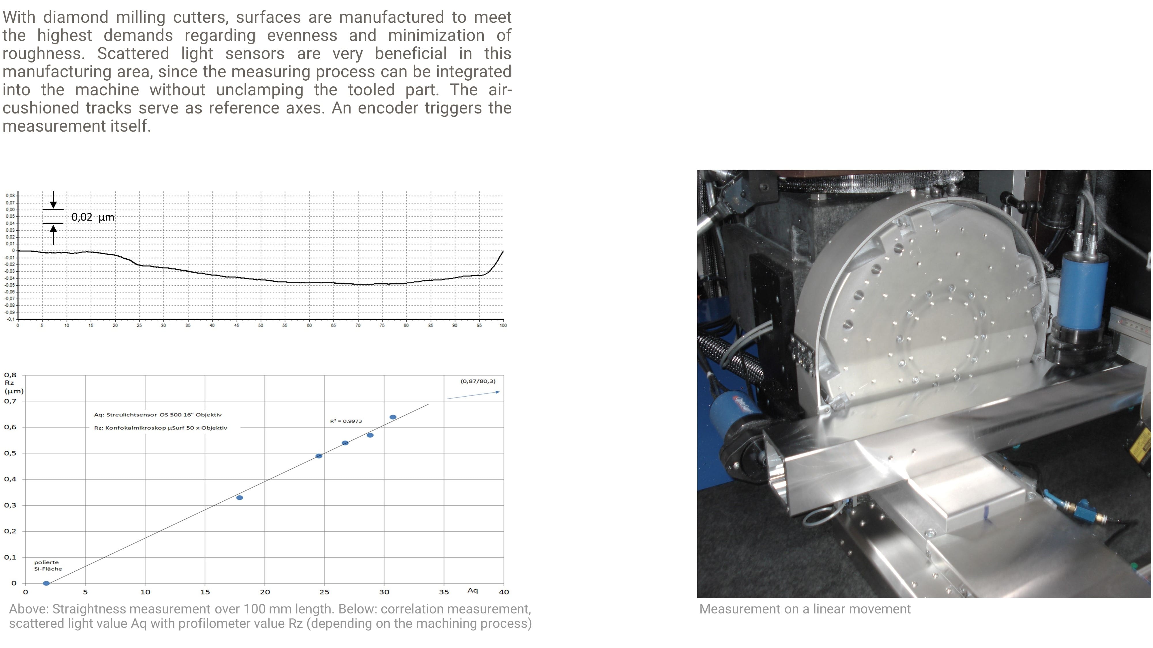
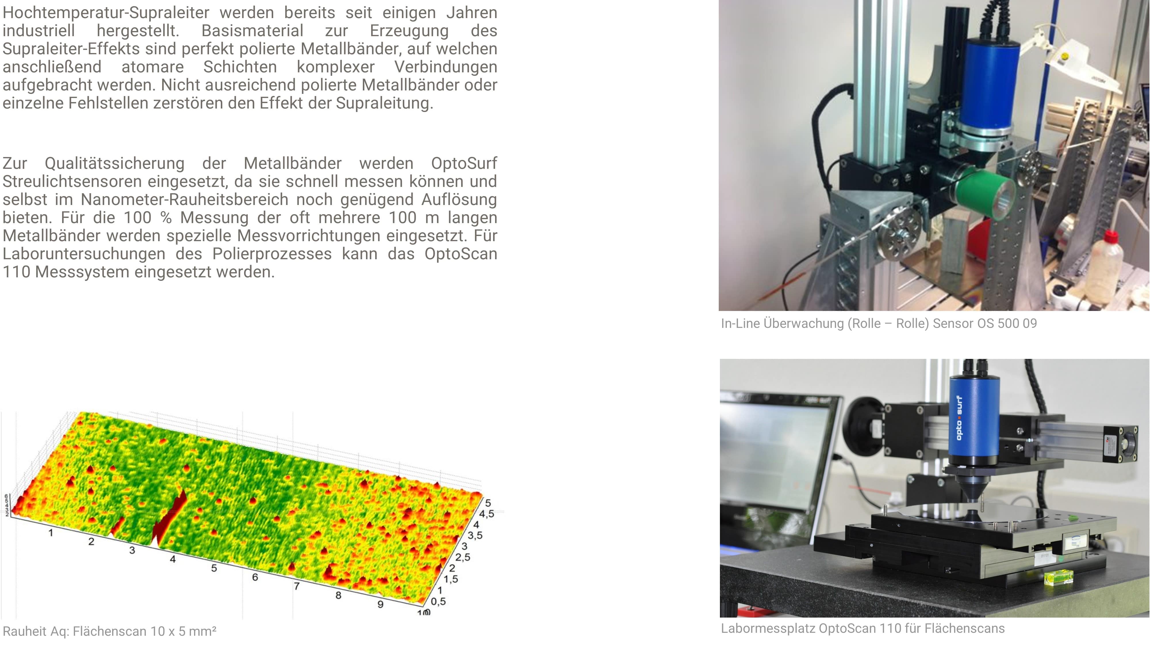
Wafer measurement machine WaferMaster
Special measuring device for the measurement of silicon wafers
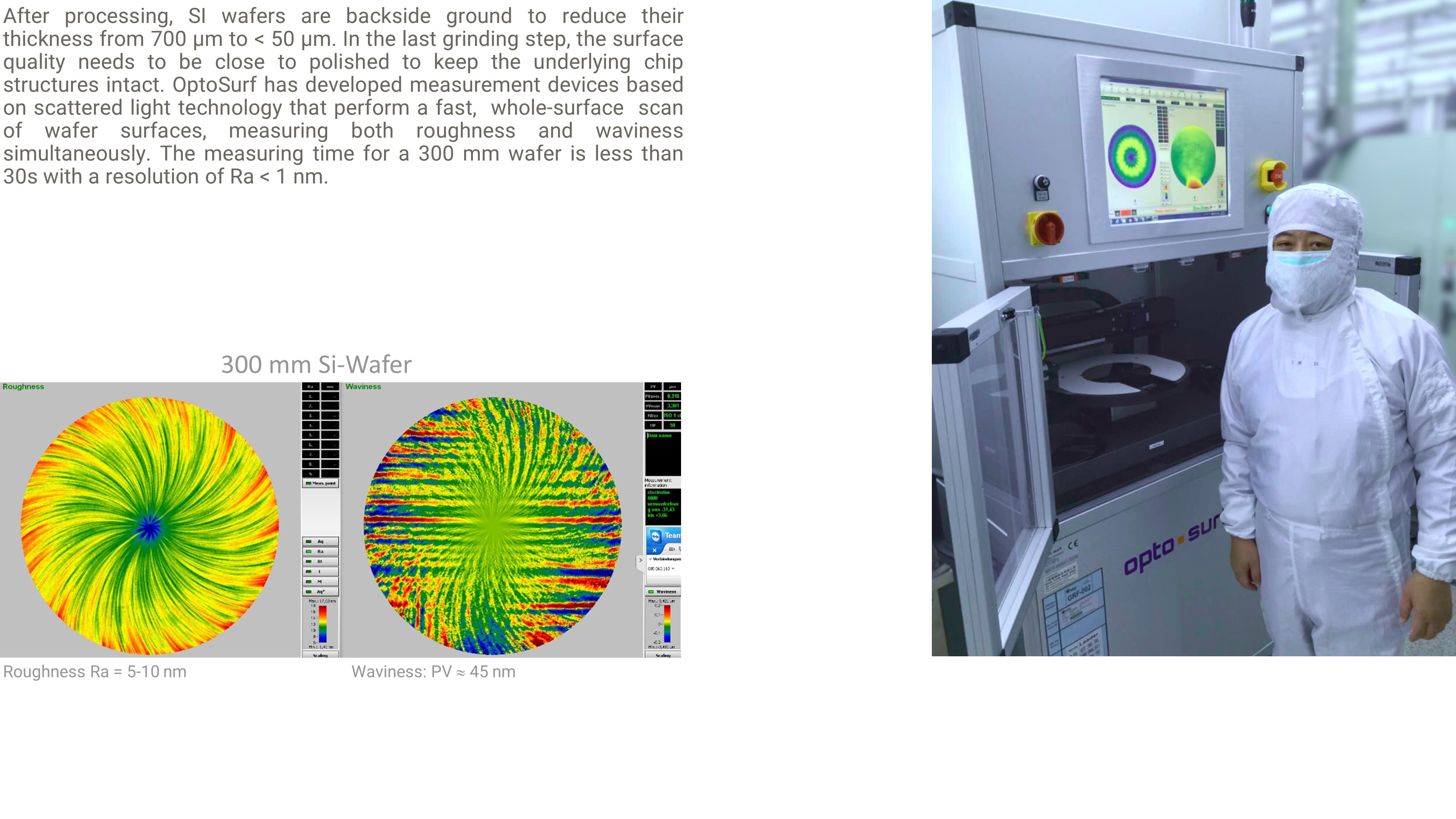
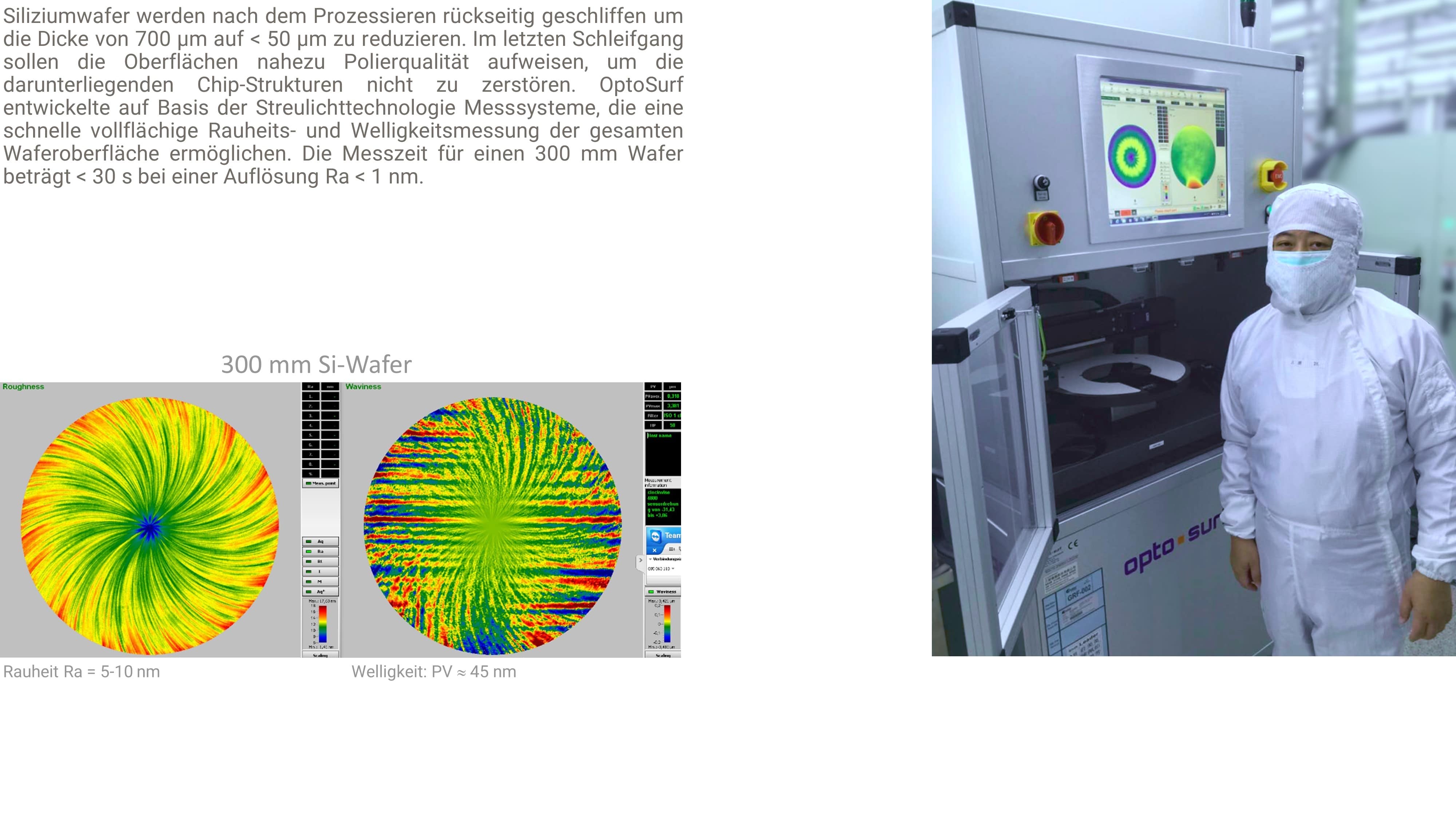
The scattered light method has been part of the semiconductor industry for many years, especially in front end. OptoSurf has been able to apply its vast experience with scattered light sensors to uses on semiconductor surfaces. The main application in the back end area is the measurement of roughness and waviness on backside ground silicon wafers. Nowadays wafers are thinned to less than 50 µm thickness by backside grinding. After polishing the roughness should be no more than Ra = 1 – 3 nm.
Using the OS 500 sensor, a rotating vacuum-chuck and a linear sensor movement, 12″ wafers are fully scanned in less than 30 seconds. Correlation functions show that the measurements completely match with white light interferometers or confocal microscopes. Measuring whole wafer surfaces with the WaferMaster measuring device has the advantage that local roughness differences are made visible, and warpage (macro geometry), as well as waviness (nano topography), are measured at the same time.